
HBM localization strategy succeeds only when capacity becomes a learning system. SK hynix’s Indiana investment should not be judged as an isolated U.S. factory. Its strategic value depends on linking Korean wafer production, U.S. advanced packaging and testing, Purdue research, local supplier qualification, and customer co-design. Localization without rapid yield and qualification feedback is construction; localization with a closed learning loop can create resilience and product advantage.
This distinction matters because high-bandwidth memory is not a commodity module assembled after the important engineering is finished. Its performance depends on the interaction among memory dies, stacking, bonding, interconnect, thermal behavior, test coverage, yield, and the customer’s accelerator or package architecture. A geographically distributed operation works only if information travels faster than the physical distance adds friction.
What Changed in SK hynix’s HBM Localization Strategy
SK hynix said it held a groundbreaking ceremony on 27 August for an advanced-packaging facility in West Lafayette, Indiana, representing an investment of more than $4 billion. The company says the site will receive HBM wafers manufactured in Korea, perform advanced packaging and testing in Indiana, complete a cleanroom by October 2028, and begin mass production in the second half of 2029. These dates and benefits are company plans, not completed outcomes. SK hynix groundbreaking announcement
The same announcement says the project will include an R&D testbed with Purdue University, is considering cooperation with more than 100 suppliers, and is expected by the company to support about 7,000 direct and indirect jobs, including roughly 1,000 workers during commercial operations. Those employment numbers are forward-looking company estimates and should be treated as such. SK hynix project and workforce details
Reuters reported that HBM4E output at the Indiana site is expected in the third quarter of 2029 and that Chief Executive Kwak Noh-Jung expects the memory shortage to continue through the end of 2030. Reuters also cited Counterpoint Research estimates that SK hynix held 58% of global HBM revenue in the first quarter of 2026. The shortage horizon and future output are forecasts, not certainties. Reuters report on Indiana output and market context
Why HBM Localization Strategy Matters Now
AI infrastructure demand has made HBM availability, package integration, and qualification timing strategic constraints. The business risk is no longer limited to whether enough memory dies can be fabricated. A product can miss its customer window if stacking yield is unstable, thermal behavior forces redesign, test escapes appear late, or the memory package cannot be qualified with a new accelerator platform on schedule.
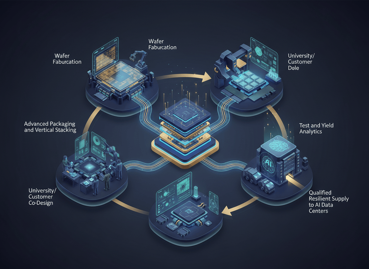
The Indiana project moves part of that critical packaging and testing capability closer to U.S. AI customers and research talent while keeping wafer production in Korea. My interpretation is that this is a deliberately distributed architecture: retain the scale and process learning of the existing wafer network, then add a customer-proximate node for packaging, validation, research, and ecosystem development. That can improve resilience only if the nodes share data, engineering priorities, and decision rights.
The Mechanism: A Five-Stage HBM Learning Loop
The first stage is wafer fabrication in Korea. Die quality, process variation, wafer-level test, and binning decisions set the starting conditions for package yield. The Indiana site therefore needs digital traceability that preserves the relationship among wafer lot, die characteristics, package configuration, equipment history, and final test outcome.
The second stage is advanced packaging. Stacking more memory dies raises alignment, bonding, warpage, interconnect, and thermal-management challenges. The important metric is not merely installed tool capacity; it is stable good-unit output at the performance and power targets required by customers. Learning-cycle time—how quickly defects are detected, attributed, corrected, and prevented—should be an executive metric.
The third stage is validation. HBM packages must survive electrical, thermal, mechanical, and reliability tests under realistic operating conditions. TrendForce’s summary of Hot Chips 2026 notes that SK hynix has evaluated packaging-platform trade-offs, including mechanical and thermal stresses across alternatives such as CoWoS variants and Intel EMIB. The report is secondary and should be read as evidence of active architecture evaluation, not a final product commitment. TrendForce summary of HBM packaging trade-offs
The fourth stage is customer and research co-design. A Purdue-linked R&D testbed can connect materials, tools, packaging methods, device characterization, and workforce development. Customer proximity can shorten the loop between package behavior and accelerator-system requirements. The value appears when research hypotheses reach pilot equipment, production data reaches researchers, and product decisions change faster—not merely when institutions share a campus.
The fifth stage is qualified supply. Volume matters only after customers approve the product and the operation can deliver repeatable quality, cost, and schedule. Qualification feedback must then return to wafer, package, test, and design teams. That closes the loop and allows the distributed system to learn as one enterprise rather than as a sequence of handoffs.
Schedule Changes Reveal the Real Execution Risk
When the investment was first announced in April 2024, Purdue described a plan to begin production in the second half of 2028. The current SK hynix timetable places mass production in the second half of 2029. The sources do not specify one cause for the change, so it would be incorrect to infer a particular delay mechanism. The updated schedule nevertheless illustrates a basic truth: semiconductor localization is a multi-year execution program exposed to permitting, construction, equipment, workforce, process-transfer, and customer-qualification risk. Purdue 2024 project announcement
Leaders should separate four milestones that are often compressed into one headline: building completion, cleanroom readiness, tool installation and process qualification, and customer-qualified mass production. Each removes a different risk. A cleanroom opening does not mean sellable output, and initial output does not mean the learning curve has reached economic yield.
The operating model also needs a single learning owner. Site leaders will optimize local output, product teams will prioritize customer commitments, and research teams will pursue longer-horizon experiments. Without a shared cadence for reviewing yield excursions, qualification failures, experiment results, and design changes, distributed expertise can become distributed accountability. A cross-site technical council should own the learning backlog and the rules for propagating validated changes.
Three Strategic Implications
- Resilience should be measured by recoverable throughput and qualification options, not the number of domestic buildings. A second geographic node creates value only when it can receive inputs, operate tools, access critical suppliers, and ship qualified output during disruption.
- Packaging data becomes a strategic asset. Lot genealogy, defect signatures, thermal maps, equipment conditions, and customer-test feedback must be governed as a shared learning layer across countries and organizations.
- The supplier ecosystem must be designed around learning velocity. Local suppliers need qualification paths, common data expectations, change-control discipline, and access to engineering feedback—not merely procurement opportunities.
Counterargument and Limits
A reasonable counterargument is that geographic distribution adds cost, duplicates capability, complicates intellectual-property protection, and slows decisions across time zones. Concentrating advanced packaging near existing wafer operations can maximize scale and engineering density. The Indiana site also will not remove dependence on Korean wafer production or globally sourced equipment and materials.
Those constraints mean localization should not be sold as self-sufficiency. The more credible objective is selective resilience: add a qualified packaging and test node near customers, build research and supplier options, and maintain interoperable process knowledge. The investment’s returns will depend on future HBM demand, execution against the 2029 schedule, customer qualification, cost competitiveness, and the durability of current market tightness.
Five Actions for Semiconductor Leaders
- Create one cross-site yield-learning system with common lot genealogy, defect taxonomy, experiment records, and escalation rules.
- Measure schedule by cleanroom, tool, process, reliability, and customer-qualification gates rather than one mass-production date.
- Assign explicit decision rights for process transfer, recipe changes, customer exceptions, supplier substitutions, and intellectual-property access.
- Qualify critical local suppliers through staged pilots and shared quality data while preserving alternate global sources for constrained inputs.
- Track learning-cycle time, qualified good-unit output, customer approval lead time, recovery time, and total delivered cost—not only announced capacity and capital spending.
Conclusion
SK hynix’s Indiana facility can become strategically important because it connects advanced packaging, testing, research, suppliers, and AI customers to an established wafer network. But a building does not create resilience by itself. The decisive capability is the feedback loop that turns defects, test results, customer requirements, and production variation into faster engineering decisions across sites. HBM localization strategy becomes an advantage when geography expands the enterprise’s learning system instead of fragmenting it.
FAQ
What will SK hynix produce in Indiana?
SK hynix says the site will perform advanced packaging and testing for HBM wafers manufactured in Korea, with mass production planned for the second half of 2029.
Why is advanced packaging critical for HBM?
HBM performance and yield depend on stacking, bonding, interconnect, thermal behavior, testing, and integration with customer accelerator packages, not only on memory-die fabrication.
Does the Indiana facility make the HBM supply chain self-sufficient?
No. It adds a U.S. packaging, testing, and R&D node but still depends on Korean wafer production and globally sourced equipment, materials, and customer qualification.
How should leaders measure localization success?
Track qualified good-unit output, yield-learning speed, customer approval lead time, supplier qualification, recovery capability, and total delivered cost rather than construction milestones alone.
References
- SK hynix. SK hynix Holds Groundbreaking Ceremony for HBM Production Base in Indiana, ‘Beginning a New Future for US-Korea AI’. SK hynix Newsroom, 28 August 2026.
- Kenrick Cai and Heekyong Yang. SK Hynix to Start AI Chip Output in Indiana in 2029, Sees Memory Shortage Through 2030. Reuters, 27 August 2026.
- Purdue University. SK hynix Announces Semiconductor Advanced Packaging Investment in Purdue Research Park. Purdue University News, 3 April 2024.
- TrendForce. Hot Chips 2026: Samsung’s zHBM Claims 70% Power-Efficiency Gain; SK hynix Evaluates Intel EMIB. TrendForce, 24 August 2026.
Related reading
- Semiconductor Industry
- From Pilot to Production: A 90-Day Roadmap for Manufacturing AI Agents
- Why AI Pilots Scale Activity but Not P&L Value
Have a question or an idea for a research or industry collaboration? Get in touch with Industry AI Decision.
Leave a Reply